ESP8266
来自Jack's Lab
(版本间的差异)
小 (→MCU 体系结构) |
(→MCU 结构) |
||
| 第30行: | 第30行: | ||
;; Tensilica Xtensa LX3 32-bit RISC SOC clocked at 80 MHz,It can also reach a maximum value of 160MHz | ;; Tensilica Xtensa LX3 32-bit RISC SOC clocked at 80 MHz,It can also reach a maximum value of 160MHz | ||
| − | ;; Only 20% of MIPS has been occupied by the WiFi stack, the rest can all be used for user application programming and development | + | ;; Only 20% of MIPS has been occupied by the WiFi stack, the rest can all be used for user application programming and development |
| − | |||
| − | + | MCU Core 的框图: | |
| − | + | ||
| − | + | ||
[[文件:Tensilica-xtensalx3.jpg]] | [[文件:Tensilica-xtensalx3.jpg]] | ||
| 第46行: | 第43行: | ||
* 80 base instructions | * 80 base instructions | ||
| − | The Xtensa ISA employs 24-bit instructions with 16-bit narrow encodings for the most common instructions. | + | The Xtensa ISA employs 24-bit instructions with 16-bit narrow encodings for the most common instructions |
| + | |||
| + | <br><br> | ||
| + | |||
| + | === SoC 内部存储 === | ||
| + | |||
| + | ESP8266EX WiFi SoC is embedded with memory controller, including SRAM and ROM. MCU can visit the memory units through iBus, dBus, and AHB interfaces. | ||
| + | |||
| + | According to our current version of SDK provided, SRAM space that is available to users is assigned as below: | ||
| + | |||
| + | * RAM size is around 50 KB, that is to say, when ESP8266EX is working under the station mode (WiFi) and is connected to the router, programmable space accessible to user in heap and data section is around 50 KB) | ||
| + | |||
| + | * There is no programmable ROM in the SoC, therefore, user program must be stored in an external SPI flash. | ||
2015年9月23日 (三) 14:28的版本
目录 |
1 概述
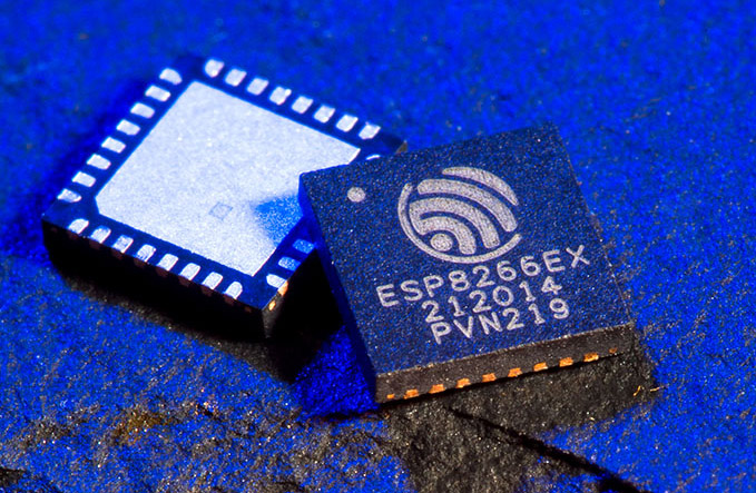
ESP8266 是一个带完整 WiFi 功能、 同时带一个 32bit MCU 的 SoC,可以取代原 Arduino 核心板 + WiFi 扩展板完成的大部分应用
最重要的,他的价格,只有 RMB 10 块左右
带 1MB Flash 的模块价格,也只在 RMB 13 块左右,批量的价格更便宜
1.1 总体结构
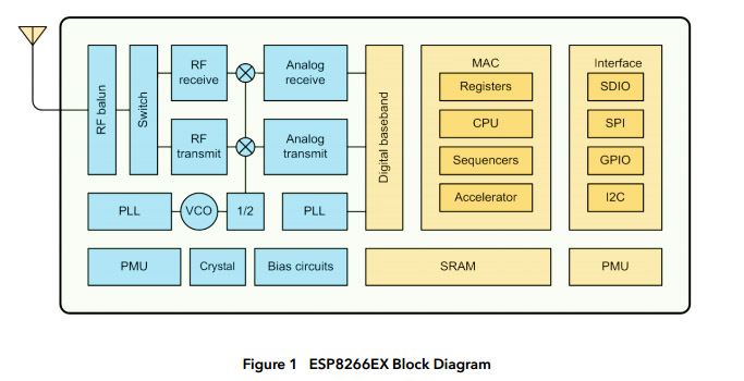
ESP8266EX 集成:天线开关,RF balun,功率放大器,低噪放大器,过滤器,电源管理模块,32 位 MCU
仅需 7 个外围器件,就是一个完整的带 32bit MCU、完整 WiFi 功能的 SoC
ESP8266 结构框图:
内部 CPU (MCU) 使用 Tensilica’s L106 钻石系列32位内核处理器,带片上 SRAM
1.2 MCU 结构
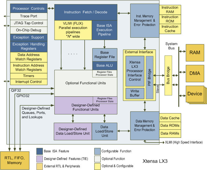
- Tensilica Xtensa LX3 32-bit RISC SOC clocked at 80 MHz,It can also reach a maximum value of 160MHz
- Only 20% of MIPS has been occupied by the WiFi stack, the rest can all be used for user application programming and development
MCU Core 的框图:
- 32-bit ALU
- 16, 32 or 64 GPR
- six special purpose registers
- 80 base instructions
The Xtensa ISA employs 24-bit instructions with 16-bit narrow encodings for the most common instructions
1.3 SoC 内部存储
ESP8266EX WiFi SoC is embedded with memory controller, including SRAM and ROM. MCU can visit the memory units through iBus, dBus, and AHB interfaces.
According to our current version of SDK provided, SRAM space that is available to users is assigned as below:
- RAM size is around 50 KB, that is to say, when ESP8266EX is working under the station mode (WiFi) and is connected to the router, programmable space accessible to user in heap and data section is around 50 KB)
- There is no programmable ROM in the SoC, therefore, user program must be stored in an external SPI flash.
2 Quick Start
3 资源


