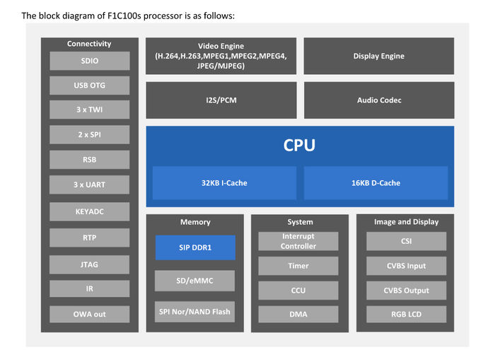
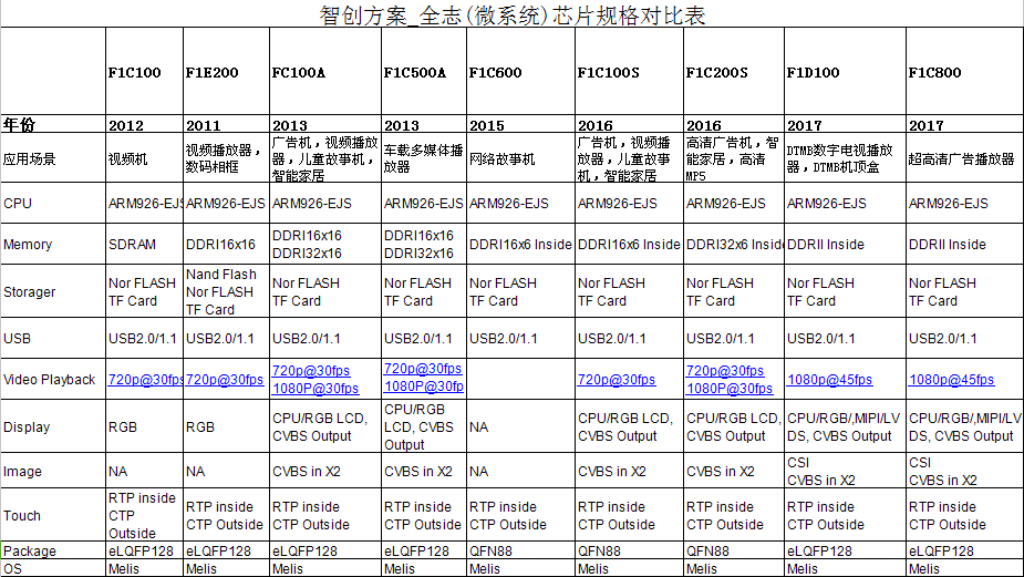
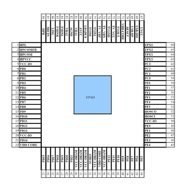
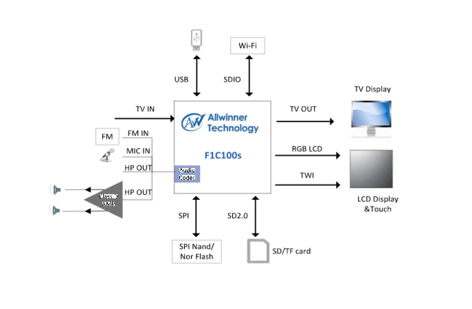
F1C
(→Overview) |
(→Typical App) |
||
| 第20行: | 第20行: | ||
[[文件:F1C100s-typical-app.jpg]] | [[文件:F1C100s-typical-app.jpg]] | ||
| + | |||
| + | <br> | ||
| + | |||
| + | == Boot == | ||
| + | |||
| + | After power-up, the F1C100s starts to fetch instructions from address 0xffff0000 which is where the BROM is located at. It's an internal integrated 32 KB ROM Chip (Boot ROM or BROM). | ||
| + | |||
| + | The BROM split up into two parts: The first part (at 0xffff0000) is the FEL mode and the second is the eGON.BRM (located at 0xffff4000). | ||
| + | |||
| + | The reset vector is located at the very begining of FEL mode: at address 0xffff0000. On reset, it jumps to 0xffff0028 where it loads 0xffff4000 (eGON.BRM) into the program counter to be executed next. | ||
| + | |||
| + | === eGON Boot === | ||
| + | |||
| + | The [[eGON#eGON.BRM|eGON Boot ROM]] performs a few tasks: | ||
| + | |||
| + | # does some [https://github.com/hno/Allwinner-Info/blob/master/BROM/ffff4000.s#L19 co-processor setup] ([http://infocenter.arm.com/help/index.jsp?topic=/com.arm.doc.ddi0344k/Bgbciiaf.html c15], (virtual) System Control Coprocessor). | ||
| + | # [https://github.com/hno/Allwinner-Info/blob/master/BROM/ffff4000.s#L23 disables] the [[TIMER#TMR_WDT_MODE|WatchDog Timer]] | ||
| + | # [https://github.com/hno/Allwinner-Info/blob/master/BROM/ffff4000.s#L28 setups] [[A10/CCM#CCM_CPU_AXI_AHB_APB0_CFG|CPU, AXI, AHB and APB0 clocks]] | ||
| + | # [https://github.com/hno/Allwinner-Info/blob/master/BROM/ffff4000.s#L34 enables] [[A10/CCM#CCM_AHB_GATING0|AHB Gating]] | ||
| + | # [https://github.com/hno/Allwinner-Info/blob/master/BROM/ffff4000.s#L38 enables] [[A10/CCM#CCM_APB0_GATING|APB0 Gating]] | ||
| + | # [https://github.com/hno/Allwinner-Info/blob/master/BROM/ffff4000.s#L40 sets] the Stack Pointer to 32K | ||
| + | # then it [https://github.com/hno/Allwinner-Info/blob/master/BROM/ffff4000.s#L41 jumps] to [https://github.com/hno/Allwinner-Info/blob/master/BROM/ffff4000.s#L84 'boot'] which immediately [https://github.com/hno/Allwinner-Info/blob/master/BROM/ffff4000.s#L86 jumps to] [https://github.com/hno/Allwinner-Info/blob/master/BROM/ffff4000.s#L2551 check_uboot] | ||
| + | # [https://github.com/hno/Allwinner-Info/blob/master/BROM/ffff4000.s#L2551 check_uboot] setups up some registers, then [https://github.com/hno/Allwinner-Info/blob/master/BROM/ffff4000.s#L2560 checks the status pin] (often called FEL pin, BSP pin or '''uboot''') | ||
| + | ## if the pin is low (connected to GND) [https://github.com/hno/Allwinner-Info/blob/master/BROM/ffff4000.s#L90 executes] [[FEL]] mode at 0xffff0020. | ||
| + | ## If the pin is high it continues trying to boot from the following media and on failure continues to the next in order. | ||
| + | ### [https://github.com/hno/Allwinner-Info/blob/master/BROM/ffff4000.s#L91 SD Card0] also known as [[A10/CCM#CCM_MMC0_CLK|MMC0]] | ||
| + | ### [https://github.com/hno/Allwinner-Info/blob/master/BROM/ffff4000.s#L98 Internal NAND flash] also known as [[A10/CCM#CCM_NAND_CLK|NAND]] | ||
| + | ### [https://github.com/hno/Allwinner-Info/blob/master/BROM/ffff4000.s#L104 SD Card2] also known as [[A10/CCM#CCM_MMC2_CLK|MMC2]] | ||
| + | ### [https://github.com/hno/Allwinner-Info/blob/master/BROM/ffff4000.s#L111 SPI connected NOR flash] also known as [[A10/CCM#CCM_SPI0_CLK|SPI]] | ||
| + | ### [https://github.com/hno/Allwinner-Info/blob/master/BROM/ffff4000.s##L117 If all fails], [[FEL/USBBoot|FEL/USB Boot]] mode is [https://github.com/hno/Allwinner-Info/blob/master/BROM/ffff4000.s#L120 executed] from 0xffff0020 | ||
| + | |||
| + | As can be seen, the SoC has several ways to boot and a lot would need to go wrong or 'fail' before entering [[FEL/USBBoot|FEL mode]]. This is especially important if there is a valid header in the NAND flash. Obviously this can be abused, by corrupting the header and thus forcing failure. If no other boot options are available, then FEL mode should be the final result. As a bypass mechanism, the A10 has the so called ''Boot Select Pin (BSP)''. This pin is normally internally pulled up by a 50KΩ resistor. If the pin is pulled low to GND, the A10 will try to boot into [[FEL/USBBoot|FEL mode]]. Otherwise the above boot-order will be tried. | ||
<br> | <br> | ||
2018年10月23日 (二) 00:15的版本
目录 |
1 Overview
2 Roadmap
3 Pinmap
4 Typical App
5 Boot
After power-up, the F1C100s starts to fetch instructions from address 0xffff0000 which is where the BROM is located at. It's an internal integrated 32 KB ROM Chip (Boot ROM or BROM).
The BROM split up into two parts: The first part (at 0xffff0000) is the FEL mode and the second is the eGON.BRM (located at 0xffff4000).
The reset vector is located at the very begining of FEL mode: at address 0xffff0000. On reset, it jumps to 0xffff0028 where it loads 0xffff4000 (eGON.BRM) into the program counter to be executed next.
5.1 eGON Boot
The eGON Boot ROM performs a few tasks:
- does some co-processor setup (c15, (virtual) System Control Coprocessor).
- disables the WatchDog Timer
- setups CPU, AXI, AHB and APB0 clocks
- enables AHB Gating
- enables APB0 Gating
- sets the Stack Pointer to 32K
- then it jumps to 'boot' which immediately jumps to check_uboot
- check_uboot setups up some registers, then checks the status pin (often called FEL pin, BSP pin or uboot)
- if the pin is low (connected to GND) executes FEL mode at 0xffff0020.
- If the pin is high it continues trying to boot from the following media and on failure continues to the next in order.
- SD Card0 also known as MMC0
- Internal NAND flash also known as NAND
- SD Card2 also known as MMC2
- SPI connected NOR flash also known as SPI
- If all fails, FEL/USB Boot mode is executed from 0xffff0020
As can be seen, the SoC has several ways to boot and a lot would need to go wrong or 'fail' before entering FEL mode. This is especially important if there is a valid header in the NAND flash. Obviously this can be abused, by corrupting the header and thus forcing failure. If no other boot options are available, then FEL mode should be the final result. As a bypass mechanism, the A10 has the so called Boot Select Pin (BSP). This pin is normally internally pulled up by a 50KΩ resistor. If the pin is pulled low to GND, the A10 will try to boot into FEL mode. Otherwise the above boot-order will be tried.
6 Reference


