F1C
(→Reference) |
(→Boot) |
||
| 第38行: | 第38行: | ||
[[文件:F1C100s-typical-app.jpg]] | [[文件:F1C100s-typical-app.jpg]] | ||
| + | |||
| + | <br> | ||
| + | |||
| + | == Quick Start == | ||
| + | |||
| + | <source lang=bash> | ||
| + | $ wget http://releases.linaro.org/components/toolchain/binaries/7.2-2017.11/arm-linux-gnueabi/gcc-linaro-7.2.1-2017.11-x86_64_arm-linux-gnueabi.tar.xz | ||
| + | $ tar -vxJf gcc-linaro-7.2.1-2017.11-x86_64_arm-linux-gnueabi.tar.xz | ||
| + | |||
| + | $ git clone -b f1c100s-spiflash https://github.com/Icenowy/sunxi-tools.git | ||
| + | $ cd sunxi-tools | ||
| + | $ make && sudo make install | ||
| + | </source> | ||
| + | |||
| + | 如果出现:fel_lib.c:26:20: fatal error: libusb.h: No such file or directory,那需要安装libusb: | ||
| + | |||
| + | sudo apt-get install libusb-1.0-0-dev | ||
| + | |||
| + | <source lang=bash> | ||
| + | $ git clone https://github.com/Lichee-Pi/u-boot.git | ||
| + | $ cd u-boot | ||
| + | # 切换到 Nano 分支 | ||
| + | $ git checkout nano-v2018.01 | ||
| + | # 此处告知make采用arm-linux-gnueabi下的所有交叉编译工具,目标架构为Arm,设定各项默认配置为 nano 的spiflash支持版 | ||
| + | # 若不带spi-flash的板子,请换成 licheepi_nano_defconfig | ||
| + | $ make ARCH=arm CROSS_COMPILE=arm-linux-gnueabi- licheepi_nano_spiflash_defconfig | ||
| + | </source> | ||
<br> | <br> | ||
2020年7月9日 (四) 16:32的版本
目录 |
1 F1C100s Overview
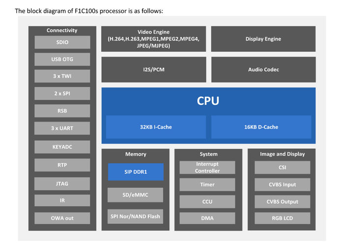
- ARM926-EJS, up to 900MHz
- 32KB I-Cache, 16KB D-Cache, 5-stage pipeline
- 32MB SiP DDR1 (F1C200s is 64MB SiP DDR1)
- RGB LCD interface
- USB 2.0 OTG
- SDIO
- SPI x2
- TWI x3
- UART x3
- TV out x 1, TV in x 2
- PWM x2
- LRADC x1
- Speaker x2 + Mic x1
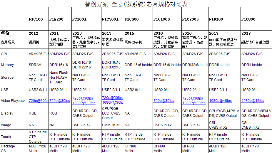
2 Roadmap
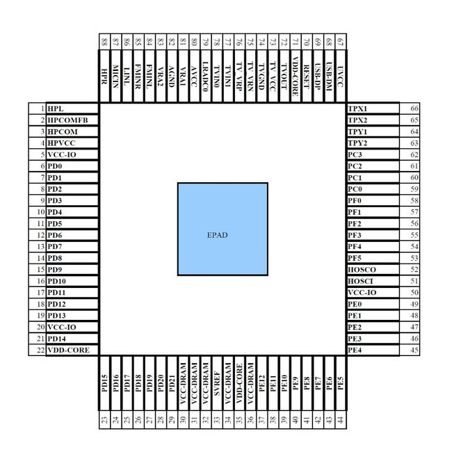
3 Pinmap
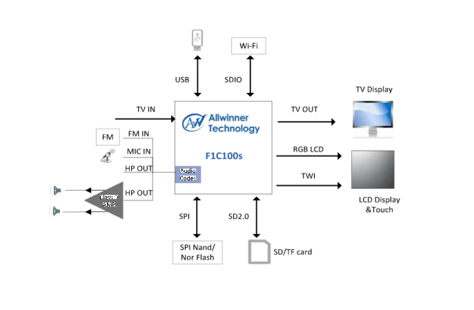
4 Typical App
5 Quick Start
$ wget http://releases.linaro.org/components/toolchain/binaries/7.2-2017.11/arm-linux-gnueabi/gcc-linaro-7.2.1-2017.11-x86_64_arm-linux-gnueabi.tar.xz
$ tar -vxJf gcc-linaro-7.2.1-2017.11-x86_64_arm-linux-gnueabi.tar.xz

$ git clone -b f1c100s-spiflash https://github.com/Icenowy/sunxi-tools.git
$ cd sunxi-tools
$ make && sudo make install
如果出现:fel_lib.c:26:20: fatal error: libusb.h: No such file or directory,那需要安装libusb:
sudo apt-get install libusb-1.0-0-dev
$ git clone https://github.com/Lichee-Pi/u-boot.git
$ cd u-boot
# 切换到 Nano 分支
$ git checkout nano-v2018.01
# 此处告知make采用arm-linux-gnueabi下的所有交叉编译工具,目标架构为Arm,设定各项默认配置为 nano 的spiflash支持版
# 若不带spi-flash的板子,请换成 licheepi_nano_defconfig
$ make ARCH=arm CROSS_COMPILE=arm-linux-gnueabi- licheepi_nano_spiflash_defconfig
6 Boot
After power-up, the F1C100s starts to fetch instructions from address 0xFFFF_0000 which is where the BROM is located at. It's an internal integrated 32 KB ROM Chip (Boot ROM or BROM).
The BROM split up into two parts: The first part (at 0xFFFF_0000) is the FEL mode and the second is the eGON.BRM (located at 0xFFFF_4000).
The reset vector is located at the very begining of FEL mode: at address 0xFFFF_0000. On reset, it jumps to 0xFFFF_0028 where it loads 0xFFFF_4000 (eGON.BRM) into the program counter to be executed next.
6.1 eGON Boot
The eGON Boot ROM performs a few tasks:
- do some co-processor setup (c15, (virtual) System Control Coprocessor).
- disables the WatchDog Timer
- setups CPU, AXI, AHB and APB0 clocks
- enables AHB Gating
- enables APB0 Gating
- sets the Stack Pointer to 32K
- then it jumps to 'boot' which immediately jumps to check_uboot
- check_uboot setups up some registers, then checks the status pin (often called FEL pin, BSP pin or uboot)
- if the pin is low (connected to GND) executes FEL mode at 0xFFFF_0020.
- If the pin is high it continues trying to boot from the following media and on failure continues to the next in order.
- SD Card0 also known as MMC0
- Internal NAND flash also known as NAND
- SD Card2 also known as MMC2
- SPI connected NOR flash also known as SPI
- If all fails, FEL/USB Boot mode is executed from 0xFFFF_0020
As can be seen, the SoC has several ways to boot and a lot would need to go wrong or 'fail' before entering FEL mode. This is especially important if there is a valid header in the NAND flash. Obviously this can be abused, by corrupting the header and thus forcing failure. If no other boot options are available, then FEL mode should be the final result. As a bypass mechanism, the A10 has the so called Boot Select Pin (BSP). This pin is normally internally pulled up by a 50KΩ resistor. If the pin is pulled low to GND, the A10 will try to boot into FEL mode. Otherwise the above boot-order will be tried.
boot-> check fel key pressed (yes)--> FEL mode (boot from USB OTG)
                          \
                      (no) \
                            \-------> 1) try to boot from SMHC0 (SD card)
                                      2) try to boot from SMHC2 (eMMC)
                                      3) try to boot from SPI0 (SPI NOR Flash)
                                      4) FEL mode (boot from USB OTG)
6.2 FEL mode
- 短接 flash 的 1、4 两脚,重新上电,上电后松开短接,即可重新进入 fel 模式
- 在启动到内核前,回车进入 uboot,执行 sf probe 0;sf erase 0 0x100000;reset 即可重新进入 fel 模式
6.3 Reference
- http://linux-sunxi.org/FEL
- http://linux-sunxi.org/FEL/USBBoot
- http://linux-sunxi.org/BROM
- http://linux-sunxi.org/Sunxi-tools
- http://nano.lichee.pro/get_started/first_eat.html#id6
7 Reference
- F1C100s Datasheet 2015
- F1C100 Datasheet 2011
- F1C600 User Manual
- Card Linux SCH
- H3 Datasheet
- V3S datasheet V3s datasheet


