Nvidia GPU Architecture
来自Jack's Lab
(版本间的差异)
(→Kepler Micro Architecture) |
(→Maxwell Micro Architecture) |
||
| 第157行: | 第157行: | ||
* 165W | * 165W | ||
| + | |||
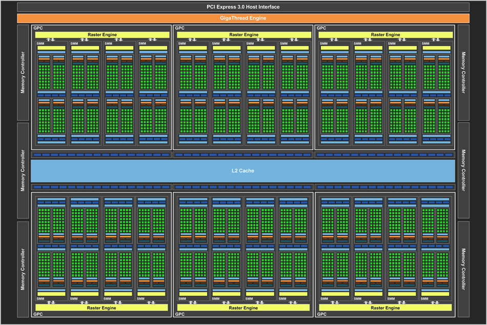
| + | TITAN X: | ||
| + | |||
| + | [[文件:TITAN-X-arch.png | 950px]] | ||
<br> | <br> | ||
2017年3月22日 (三) 16:46的版本
目录 |
1 Overview
The GPU architecture is built around a scalable array of Streaming Multiprocessors (SM)
The key components of a SM:
- CUDA cores (ALU + FPU)
- Double Precision Units (DPU)
- Special Function Units (SPU)
- Load/Store Units (LD/ST)
- Register File
- Shared Memory/L1 Cache
- Warp Scheduler
2 Fermi Micro Architecture
The Fermi architecture was the first complete GPU computing architecture to deliver the features required for the most demanding HPC applications.
- 1 CUDA core: 1 ALU + 1 FPU
- 1 SM: 32 CUDA cores + 16 Load/Store Unit + 4 SPU + 2 Warp Scheduler
- 1 SM: 2 Warps
- 1 Warp: 16 CUDA cores + 16 Load/Store Unit(shared) + 4 SPU(shared) + [32 threads context ?]
- Handle 48 warps per SM for a total of 1536 (48x32) threads resident in a single SM at a time [48 Warps context ?]
- Register file is 32KB
GTX480:
- 15 SM (32 CUDA cores/SM)
- 480 CUDA cores
- 1345 GFLOPs
- 40 nm
- 3.2 billion transistors
- GTX480 250Watts
2.1 Fermi Cards
2.1.1 GeForce 400 Series
- Release date: April 12, 2010
- Codename: GF10x
- Architecture: Fermi
- Models:
- GeForce Series
- GeForce GT Series
- GeForce GTS Series
- GeForce GTX Series
- Fabrication process and transistors:
- 260M 40nm (GT218)
- 585M 40 nm (GF108)
- 1.170M 40 nm (GF106)
- 1.950M 40 nm (GF104)
- 1.950M 40 nm (GF114)
- 3.200M 40 nm (GF100)
- Cards:
- Entry-level GT420 GT430
- Mid-range GT440 GTS450 GTX460
- High-end GTX465 GTX470
- Enthusiast GTX480 (2010.3, 3.2 billion Transistors, 15 SMs, 1536MB, 1345 GFLOPS, 250W)
2.1.2 GeForce 500 Series
- Release date: 8 November 2010
- Codename: GF11x
- Architecture: Fermi
- Models:
- GeForce Series
- GeForce GT Series
- GeForce GTX Series
- Fabrication process and transistors:
- 292M 40nm (GF119)
- 585M 40 nm (GF108)
- 1.170M 40 nm (GF116)
- 1.950M 40 nm (GF114)
- 3.000M 40 nm (GF110)
- Cards:
- Entry-level 510 GT520 GT530
- Mid-range GT545 GTX550Ti GTX560 GTX560Ti
- High-end GTX570 GTX580 GTX590(2011.3, 2x3 billion transistors, 32 SMs, 2x1536MB, 2488GFLOPS, 365W)
3 Kepler Micro Architecture
Released in the fall of 2012
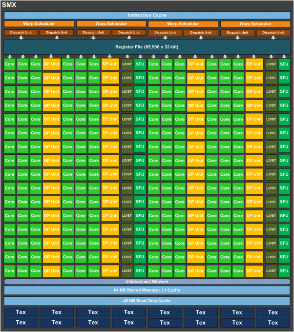
- 1 SM: 4 Warps Scheduler (2 instruction dispatchers per Warp)
- 1 Warp: [32 threads context ?]
- 1 SM: 192 CUDA cores + 64 DPU (shared) + 32 Load/Store Unit (shared) + 32 SPU (shared) + 4 Warp Scheduler
- Handle 64 warps/SM for a total of 2048 (64x32) threads resident in a single SM at a time [64 Warps context ?]
- Register file size is 64K
K20X:
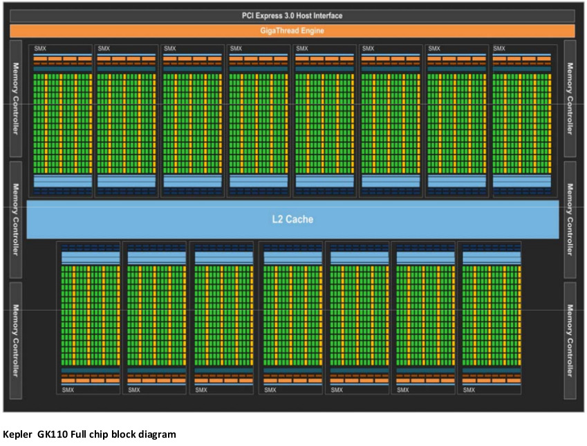
- 14 SM
- 2688 CUDA cores, 6GB
- 3.935 TFLOPs / DPU: 1.312 TFLOPs
- 28 nm
- 235Watts
GTX690:
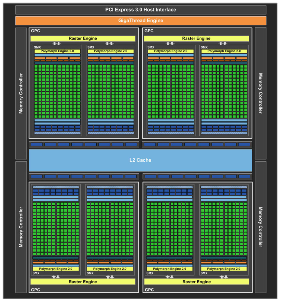
- 2x8 SM
- 3072 CUDA cores
- 2x2.8TFLOPs
- 2x3.54 billion transistors
- 300Watts (2012.4)
4 Maxwell Micro Architecture
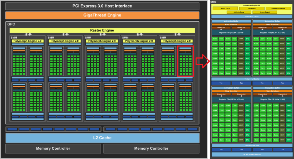
GM204:
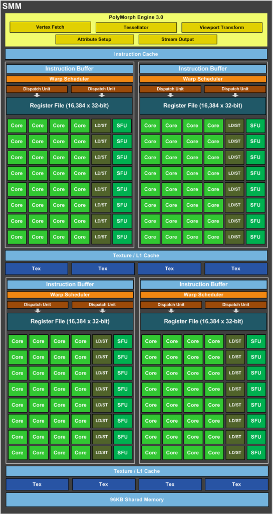
- 1 SM (SMM): 4 Warp Scheduler (2 instruction dispatchers per Warp)
- 1 Warp: 32 CUDA cores + 1 DPU + 8 Load/Store Units + 8 SPU
- 1 SM (SMM): 128 CUDA cores + 4 DPU + 32 Load/Store Units + 32 SPU
GTX980:
- 16 SM (SMM)
- 2048 CUDA cores
- 4612 GFLOPs / DPU: 144 GFLOPs
- 28 nm
- 5.2 billion transistors
- 165W
TITAN X:
5 Reference
- https://en.wikipedia.org/wiki/Fermi_(microarchitecture)
- https://en.wikipedia.org/wiki/GeForce_400_series
- https://en.wikipedia.org/wiki/GeForce_500_series
