Xtensa L106 Architecture
来自Jack's Lab
(版本间的差异)
(以“== Overview == <br><br> == See also == <br><br> <br><br> <br><br> <br><br> <br><br> <br><br> <br><br> <br><br> <br><br> <br><br> <br><br> <br><br>”为内容创建页面) |
(→Overview) |
||
| 第1行: | 第1行: | ||
== Overview == | == Overview == | ||
| + | |||
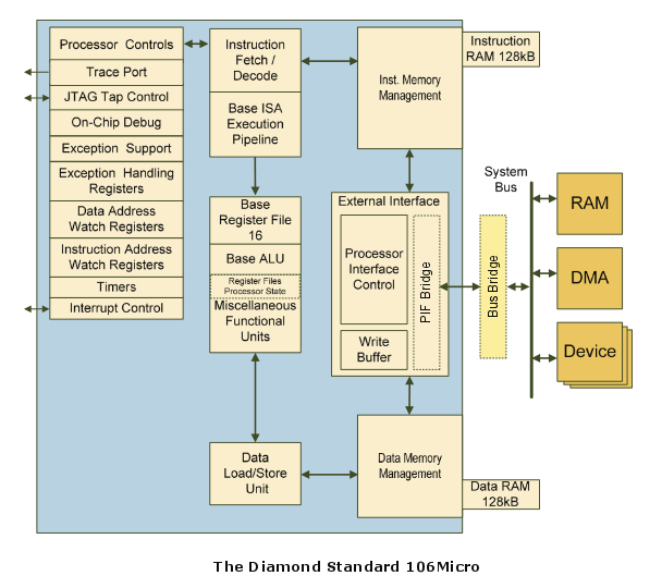
| + | [[文件:Tensilica-xtensa-l106.png]] | ||
| + | |||
| + | |||
| + | * Small, low power 32-bit RISC controller core, Xtensa ISA | ||
| + | * Cache-less processor with memory protection unit | ||
| + | * 5-stage pipeline | ||
| + | * Dhrystone 2.1: 1.22 DMIPS/MHz | ||
| + | * 24/16-bit ISA with modeless switching | ||
| + | * Iterative 32x32 multiplier | ||
| + | * Separate instruction and data memory interfaces | ||
| + | * Integrated interrupt controller with 15 interrupts at 2 priority levels | ||
| + | * 32-bit ALU | ||
| + | * 16 GPRs | ||
<br><br> | <br><br> | ||
2015年11月16日 (一) 17:35的版本
1 Overview
- Small, low power 32-bit RISC controller core, Xtensa ISA
- Cache-less processor with memory protection unit
- 5-stage pipeline
- Dhrystone 2.1: 1.22 DMIPS/MHz
- 24/16-bit ISA with modeless switching
- Iterative 32x32 multiplier
- Separate instruction and data memory interfaces
- Integrated interrupt controller with 15 interrupts at 2 priority levels
- 32-bit ALU
- 16 GPRs
2 See also
